 |
| May 25, 2021 | Volume 17 Issue 20 |
Designfax weekly eMagazine

Archives
Partners
Manufacturing Center
Product Spotlight
Modern Applications News
Metalworking Ideas For
Today's Job Shops
Tooling and Production
Strategies for large
metalworking plants
Researchers create world's most power-efficient high-speed ADC microchip
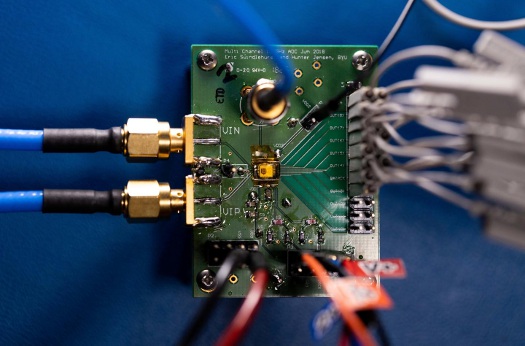
Image of an analog-to-digital converter. [Credit: BYU Photo]
To meet soaring demand for lightning-quick mobile technology, each year tech giants create faster, more powerful devices with longer-lasting battery power than previous models.
A major reason companies like Apple and Samsung can miraculously pull this off year after year is because engineers and researchers around the world are designing increasingly power-efficient microchips that still deliver high speeds.
To that end, researchers led by a team at Brigham Young University (BYU) have just built the world's most power-efficient high-speed analog-to-digital converter (ADC) microchip. An ADC is a tiny piece of technology present in almost every electronic piece of equipment that converts analog signals (like a radio wave) to a digital signal.
The ADC created by BYU professor Wood Chiang, Ph.D. student Eric Swindlehurst, and their colleagues consumes only 21 milliwatts (mW) of power at 10 GHz for ultra-wideband wireless communications; current ADCs consume hundreds of milliwatts or even Watts of power at comparable speeds. The BYU-made ADC has the highest power efficiency currently available globally, a record it holds by a substantial margin.
"Many research groups worldwide focus on ADCs; it's like a competition of who can build the world's fastest and most fuel-efficient car," Chiang said. "It is very difficult to beat everyone else around the world, but we managed to do just that."
The central challenge facing researchers like Chiang is that increasingly higher bandwidths within communications system devices means circuits that consume more power. Chiang, Swindlehurst, and their team set out to solve the problem by focusing on a key part of the ADC circuit called the DAC, which is a central piece that stands for the exact reverse of ADC: digital-to-analog converter.
How'd they do it? A technical explanation
The team made the converter faster and more efficient by reducing the loading from the DAC by scaling both the capacitor parallel plate area and spacing. They also grouped unit capacitors differently from the conventional way, grouping together unit capacitors that are part of the same bit in the DAC rather than having them be interleaved throughout. Doing so lowered the bottom-plate parasitic capacitance by three times, significantly lowering power consumption while increasing speed.
Finally, they used a bootstrapped switch, but improved on it by making it a dual-path one, where each path can be independently optimized. This method increases the speed but doesn't require additional hardware because it involves splitting existing devices and making route changes in the circuit.
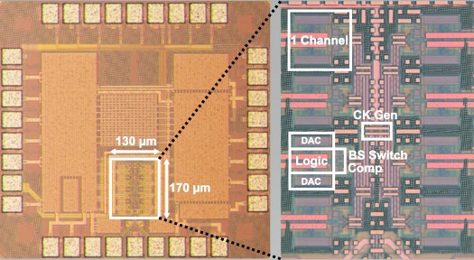
A microscopic image of the analog-to-digital converter chip created by the researchers at Brigham Young University. [Credit: Courtesy Shiuh-hua Wood Chiang]
The project, sponsored by the Ministry of Science in Taiwan and a consortium of technology companies, took four years to complete -- three years to design the chip and one year to test it. The team, which included collaborators from National Yang Ming Chiao Tung University in Taiwan and the University of California, Los Angeles, published details of the project in IEEE Journal of Solid-State Circuits earlier this year, with Swindlehurst serving as principal author.
"We've proven the technology of the chip here at BYU, and there is no question about the efficacy of this particular technique," Chiang said. "This work really pushes the envelope of what's possible and will result in a lot of conveniences for consumers. Your Wi-Fi will continue to get better because of this technology, you'll have faster upload and download speeds, and you can watch 4K or even 8K with little-to-no lag while maintaining battery life."
Chiang said other likely applications for the ADC include autonomous vehicles (which use a ton of wireless bandwidth), smart wearables like glasses or smart contact lenses, and even things such as implantable devices.
The device required sophisticated design and verification to ensure that all the thousands of connections in the converter would work correctly. A single mistake in the design would have taken at least an additional year to correct, so the team was thrilled to have made no mistakes.
"It's like building a little city. There are so many details that went into this project," Chiang said. "The student team did a marvelous job -- all the pieces fit perfectly together to realize this engineering feat. I am fortunate to have worked with such talented students at BYU."
See "An 8-bit 10-GHz 21-mW Time-Interleaved SAR ADC With Grouped DAC Capacitors and Dual-Path Bootstrapped Switch" published in IEEE Journal of Solid-State Circuits, Feb. 22, 2021.
Source: Brigham Young University
Published May 2021
Rate this article
View our terms of use and privacy policy